

300 mm Wafer FOUPs and FOSBs Are Becoming the Silent Backbone of Advanced Semiconductor Fabs by 2034
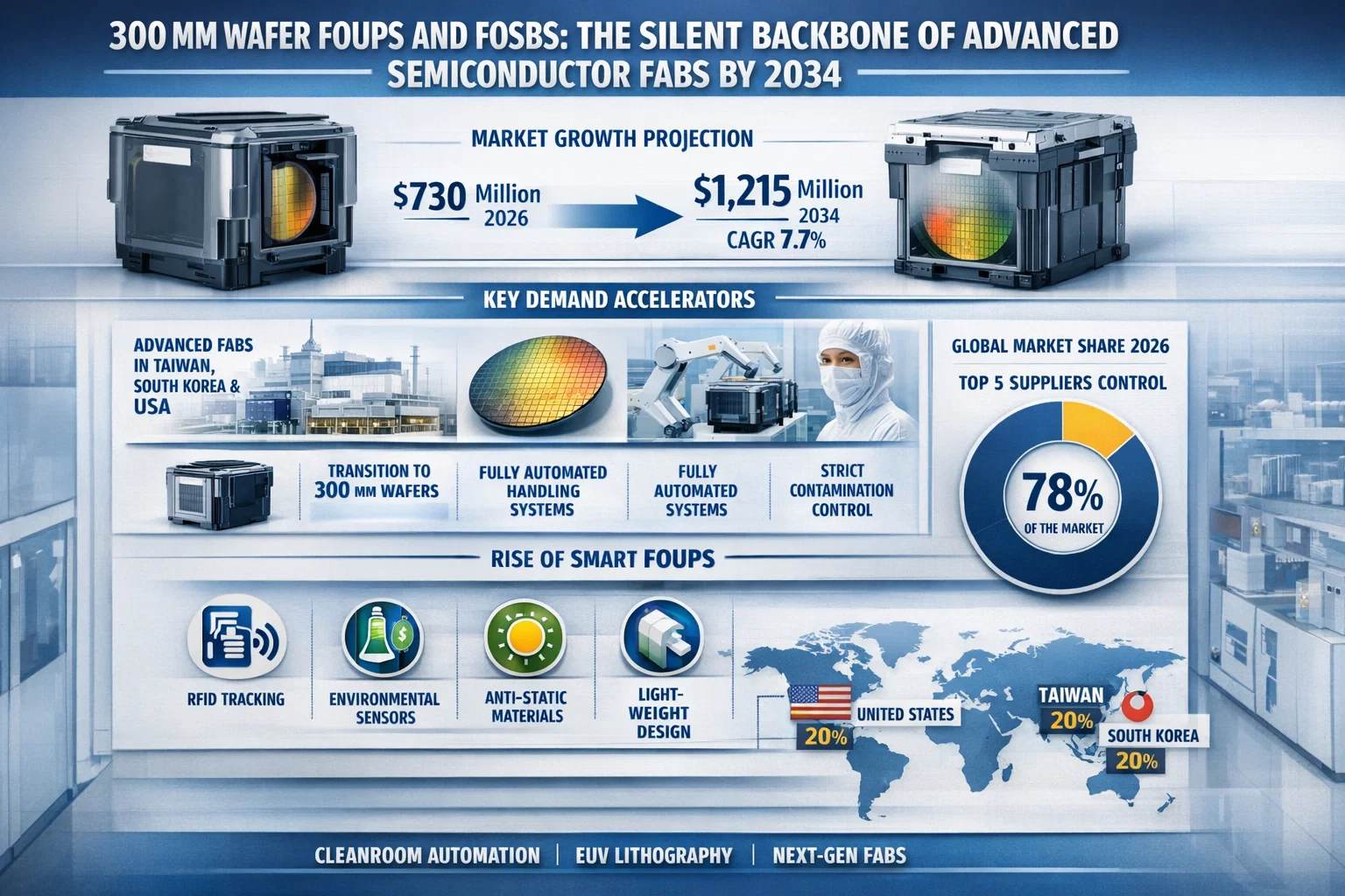
global 300 mm Wafer FOUP and FOSB market is gaining strategic importance as semiconductor manufacturers accelerate capacity expansions and automation initiatives worldwide. Valued at 730 million in 2026, the market is projected to reach 1,215 million by 2034, growing at a CAGR of 7.7 percent during the forecast period 2026–2034.
Front Opening Unified Pods (FOUPs) and Front Opening Shipping Boxes (FOSBs) are mission-critical wafer handling solutions designed to protect 300 mm silicon wafers from contamination, mechanical shock, and electrostatic discharge throughout fabrication and transportation. FOUPs enable fully automated wafer movement inside cleanrooms through robotic interfaces, while FOSBs ensure safe inter-facility shipping using advanced cushioning and shock-absorption materials.
The market’s growth trajectory is closely tied to rising 300 mm wafer adoption across foundries and integrated device manufacturers (IDMs), particularly as advanced nodes below 7 nm demand near-zero contamination environments. Taiwan and the United States remain pivotal demand centers, together accounting for nearly 40 percent of global consumption, driven by sustained investments in leading-edge fabrication facilities.
➡️ Access full market sizing, fab-level demand analysis, and competitive benchmarking
https://semiconductorinsight.com/report/300-mm-wafer-foup-and-fosb-market/
Why Demand for 300 mm Wafer Carriers Is Accelerating
As semiconductor manufacturers pursue higher yields and lower defect densities, wafer handling systems have moved from being operational necessities to strategic yield enablers. FOUPs, in particular, play a vital role in protecting wafers during lithography, etching, deposition, and inspection stages where even microscopic particles can compromise device performance.
Key demand accelerators include:
- Rapid expansion of advanced fabs in Taiwan, South Korea, and the United States
- Increasing transition from 200 mm to 300 mm wafers for cost efficiency
- Rising deployment of fully automated material handling systems (AMHS)
- Tighter contamination control requirements for EUV lithography
Industry estimates indicate that over 65 percent of semiconductor fabs were operating with fully automated wafer handling systems by 2026, up from just 35 percent a decade earlier, directly boosting FOUP adoption.
Automation and Smart FOUP Designs Reshaping the Market
Modern cleanroom environments are evolving toward Industry 4.0–enabled fabs, where wafer carriers are no longer passive containers. Advanced FOUPs now integrate:
- RFID-based wafer tracking
- Environmental monitoring sensors
- Anti-static and low-outgassing materials
- Lightweight composite designs compatible with high-speed robotics
These innovations enhance traceability, reduce downtime, and support predictive maintenance strategies, making smart FOUPs essential for next-generation fabs.
Competitive Landscape: Market Concentration Remains High
The 300 mm FOUP and FOSB market is highly consolidated, with the top five suppliers controlling approximately 78 percent of global revenue. High capital requirements, strict qualification cycles, and long-term supply agreements with leading foundries create substantial entry barriers.
Key manufacturers profiled include:
- Entegris (United States) – Advanced contamination control leader
- Shin-Etsu Polymer (Japan) – High-performance polymer solutions
- Miraial (Japan) – Precision cleanroom container specialist
- Gudeng Precision (Taiwan) – Foundry-focused carrier solutions
- Chuang King Enterprise (Taiwan) – Fast-growing regional supplier
- 3S Korea (South Korea) – Expanding presence in Asia
- Dainichi Shoji (Japan) – Niche precision component provider
While global leaders maintain dominance through sustained R&D investments, regional suppliers increasingly compete on customization speed and localized support.
Market Segmentation Snapshot
By Product Type
- FOUP (Front Opening Unified Pod)
- Standard capacity
- High-capacity
- Customized designs
- FOSB (Front Opening Shipping Box)
- Standard shipping
- Shock-resistant models
By Application
- Wafer Foundries
- Integrated Device Manufacturers (IDMs)
By Material
- Polypropylene (PP)
- Polycarbonate (PC)
- Composite and specialty materials
By Capacity
- 13-wafer capacity
- 25-wafer capacity
- Custom configurations
Regional Outlook Highlights
North America
North America remains a key growth region, supported by advanced fab construction in the United States under semiconductor manufacturing incentive programs. States such as Arizona and Texas continue to attract large-scale investments, driving demand for automation-ready FOUPs. However, suppliers face rising material costs and supply chain complexity.
Europe
Europe’s FOUP and FOSB demand is shaped by its specialized semiconductor ecosystem, particularly in Germany and France. The region emphasizes high-precision manufacturing and RFID-enabled wafer carriers, though strict environmental regulations on specialty plastics pose operational challenges.
What the Report Delivers
This report provides an in-depth assessment of the global and regional 300 mm Wafer FOUP and FOSB market across the 2026–2034 forecast horizon, including:
- Market size, volume trends, and long-term forecasts
- Detailed segmentation by type, application, material, and capacity
- Regional demand patterns and fab-level investment trends
- Competitive landscape, supplier strategies, and R&D focus areas
📊 Request a sample report to review data tables, charts, and methodology
https://semiconductorinsight.com/download-sample-report/?product_id=103384
About Semiconductor Insight
Semiconductor Insight is a global intelligence platform delivering data-driven market insights, technology analysis, and competitive intelligence across the semiconductor and advanced electronics ecosystem. Our research supports OEMs, component suppliers, investors, policymakers, and system integrators in identifying high-growth opportunities and strategic shifts shaping the future of electronics.
🌐 https://semiconductorinsight.com/
🔗 LinkedIn: Follow Semiconductor Insight
📞 International Support: +91 8087 99 2013